Brake-Light PCB
HyTech Racing – PCB Design
Overview
Designed a custom brake-light printed circuit board system which flashed LEDs when plugged into USB-C port. This project required starting each process of PCB creation from scratch: schematic symbol creation, RLC circuit layout, routing, and soldering.
Technical Details
To create the PCB I had to understand components that would execute the tasks: -LED’s on the altium library that were approved for brake-lights in FSAE -A power source to provide power to LED’s -Resistors and capacitors to alter voltage and current to match datasheet values -Timer to sequence the lighting process
LED’s were laid out by team leads as APT1608, with schematic symbol and footprint provided.
Resistor and capacitor models were also provided on the Altium Library.
Power source was chosen to be USB-C port, which can supply a broad range of voltages & currents, which will be modified in the RC layout.
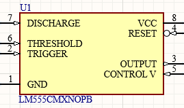
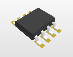
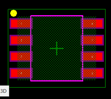
Timer was chosen to be LM555, requiring me to research the datasheet, create an associating schematic symbol and 8 short outlined integrated circuit(8-SOIC) footprint.
Design Process
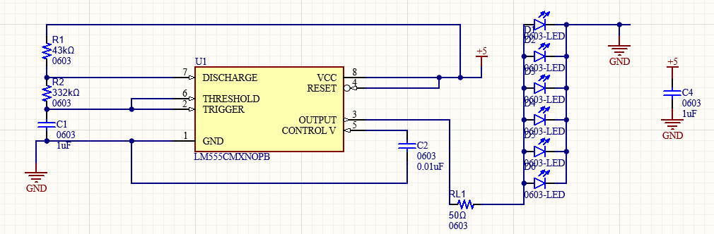
Schematic Symbol – LM555 Timer
Pin placement was driven by function. VCC and RESET are grouped together on the top right because neither cares about a precise voltage reading and just need a logic high to be active, so keeping them adjacent makes it easy to tie RESET high without long traces. THRESHOLD and TRIGGER are placed next to each other on the left because they operate on the same current thresholds (2/3 and 1/3 of VCC respectively) and work as a pair to set and reset the internal flip-flop: grouping them together reflects how they're used in the timing circuit. DISCHARGE sits just above them rather than alongside, because although it's related to the timing cycle, it sources a slightly different current path through the external RC network. OUTPUT and CONTROL VOLTAGE are placed on the right, with output prominent since it's the primary signal we care about. GND anchors the bottom left as laid out by the electric style guide. Additionally, each pin follows the type outlined on the datasheet. VCC and GND are both power pins, while DISCHARGE, THRESHOLD, TRIGGER, CONTROL V, and RESET are inputs while OUTPUT is an output.
8-SOIC Footprint
Resistor & Capacitor Circuit Layout
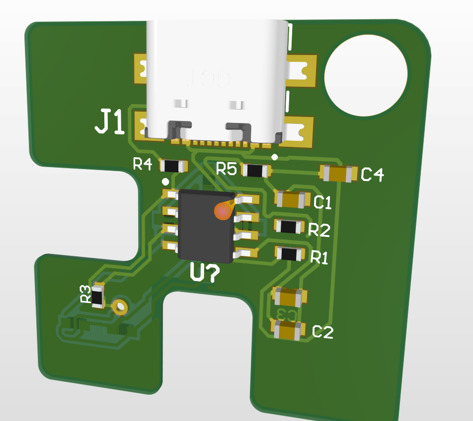
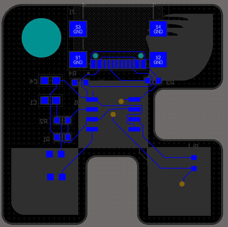
The OUTPUT pin drives six 0603 LEDs through a 50Ω current-limiting resistor (RL1), sized to keep each LED within its rated forward current at 5V. VCC and RESET are both tied directly to the +5V rail: RESET is held high so the timer runs freely without any interrupt.
C2 (0.01µF) decouples the CONTROL VOLTAGE pin, and C4 (1µF) decouples the +5V rail: both suppress noise that could otherwise affect timing stability. These are also routed near the voltage inputs on the schematic.
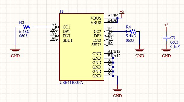
The power source is a USB4110GFA USB-C connector (J1). VBUS is wired directly to the +5V rail, and all GND and shield pins are tied to ground. The data lines (DP, DN, SBU) are left unconnected since only power is needed. R3 and R4 (both 5.1kΩ) are pull-down resistors on the CC1 and CC2 pins. C3 (0.1µF) decouples the VBUS line at the connector to filter any noise coming in from the cable.
Routing
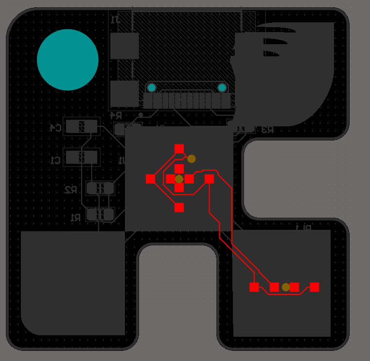
Trace width was set to 5 mil rather than the typical 10 mil since the board is small and the components are simple enough that this was sufficient. The LEDs are placed on the top layer for a clean appearance, so vias were used to bring power up from the bottom layer to the top-layer LED pads.
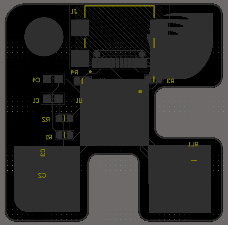
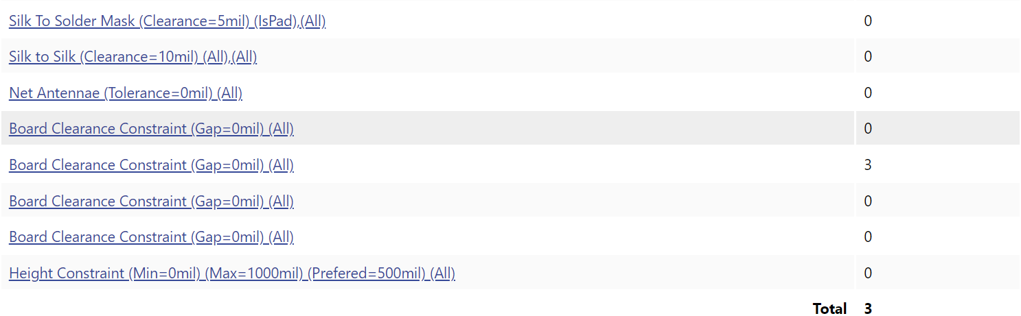
Getting to zero DRC errors required iteration. My first mistake was placing components without a routing plan, which led to conflicts that were hard to untangle. Once I shifted to a systematic approach (orient GND pads, pour GND, then route power traces inward) the process became much cleaner. A common error I hit was silk-to-solder-mask violations, where a component's reference label on the bottom overlay was overlapping a pad. These were resolved by simply relocating the labels. After working through all violations, the board passed the FSAE & HyTech DRC with 0 errors.
Outcome
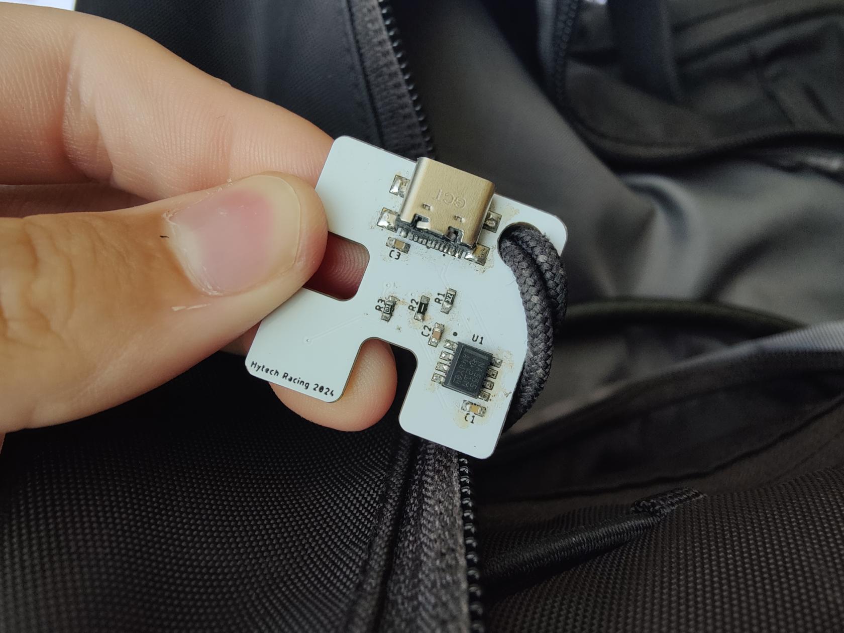
After manufacturing and soldering, the board performed exactly as designed. Plugging into a USB-C power source immediately drives the LM555 timer into astable oscillation, flashing all six LEDs at the programmed rate without any additional configuration. The physical product are visible in the photo below.