Supercapacitor IC
Circuit Design – Power Electronics
Overview
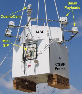
As a systems design subteam engineer of the Chip Scale Power & Energy Vertically Integrated Projects (VIP) team at Georgia Tech, I led the design of a integrated circuit for a supercapacitor characterization experiment system. The supercapacitors being tested are fabricated in-house and target space-based energy storage applications. Our fabricated supercapacitors and experimental cards will take flight on a NASA balloon in Fall 2026 inside a payload through the High Altitude Student Platform. Our circuit targets Galvanostatic Charge Discharge cycling in order to determine supercapacitor capacitance stability and resistance over time.
Technical Details
The core requirement is constant-current charge and discharge at 10µA. For charging, this means selecting a dedicated constant-current chip and ensuring safeguarding mechanisms for overcharging. For discharging, it means designing a custom subunit using components that can hold the current steady as the supercapacitor voltage drops. Because our experiment will take place in the stratosphere, we must meticulously select components rated down to -60°C.
As experiment card circuit lead, I used my prior PCB experience from HyTech Racing to guide teammates through circuit design fundamentals while building out the discharge section in KiCad.
Design Process
Constant Current Charge
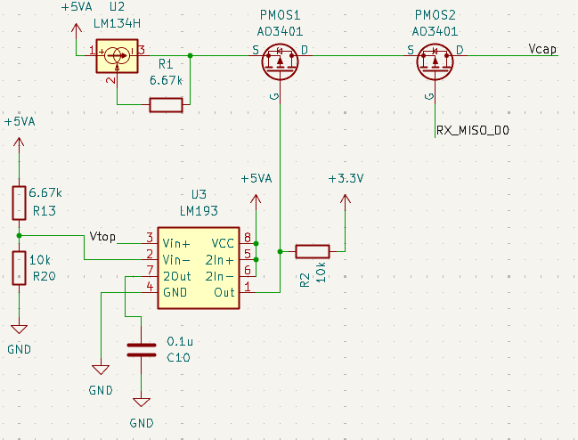
What makes this chip well suited for the task is that it internally adjusts its output to compensate for whatever resistance the path presents as its voltage rises during charging. It samples the voltage and uses internal feedback to maintain a constant current regardless of deviations in path resistance.
However, this behavior introduces a risk: once the supercapacitor is fully charged, the LM134H can drive the supercapacitor voltage above its rated limit. To prevent this, the LM193 comparator monitors the supercapacitor voltage against a 3V reference(max the supercapacitor can take). If the capacitor voltage exceeds 3V, the comparator output floats, which is pulled up to 3.3V by a pull-up resistor, opening the gate of the PMOS1 in series with the charge path and cutting off current. Below 3V, the output is pulled low, keeping the PMOS conducting.
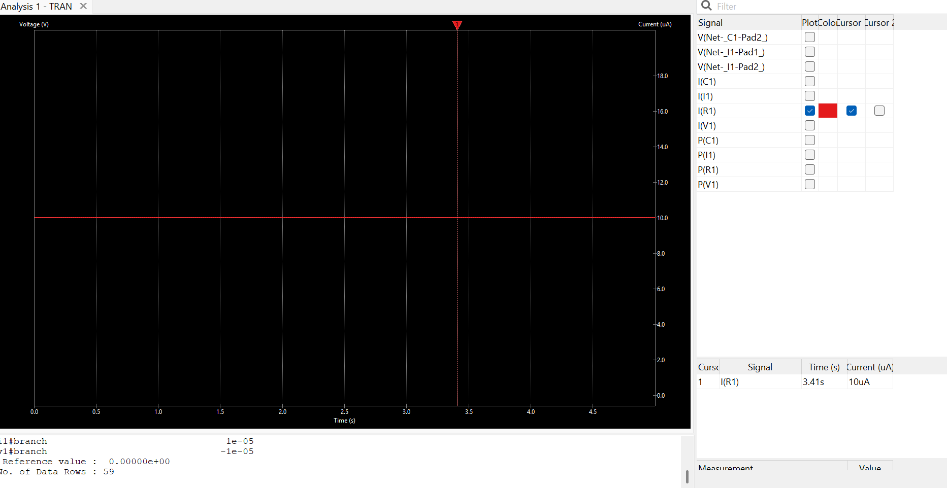
Since the LM134H relies on an external component model that KiCad's SPICE engine cannot simulate directly, running a transient analysis on the schematic produces no result. To validate the behavior, the LM134H is swapped out for an IDC set to output 10µA. This lets us confirm that a 10µA source will behave correctly with the rest of the circuit before committing to the real chip.
Constant Current Discharge
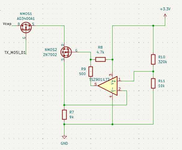
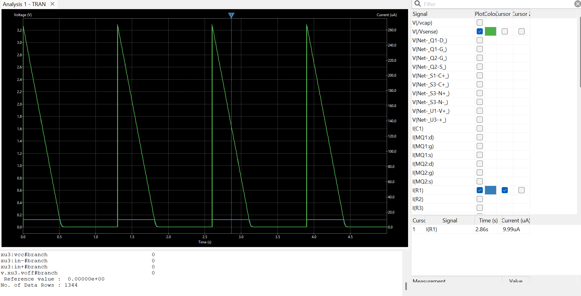
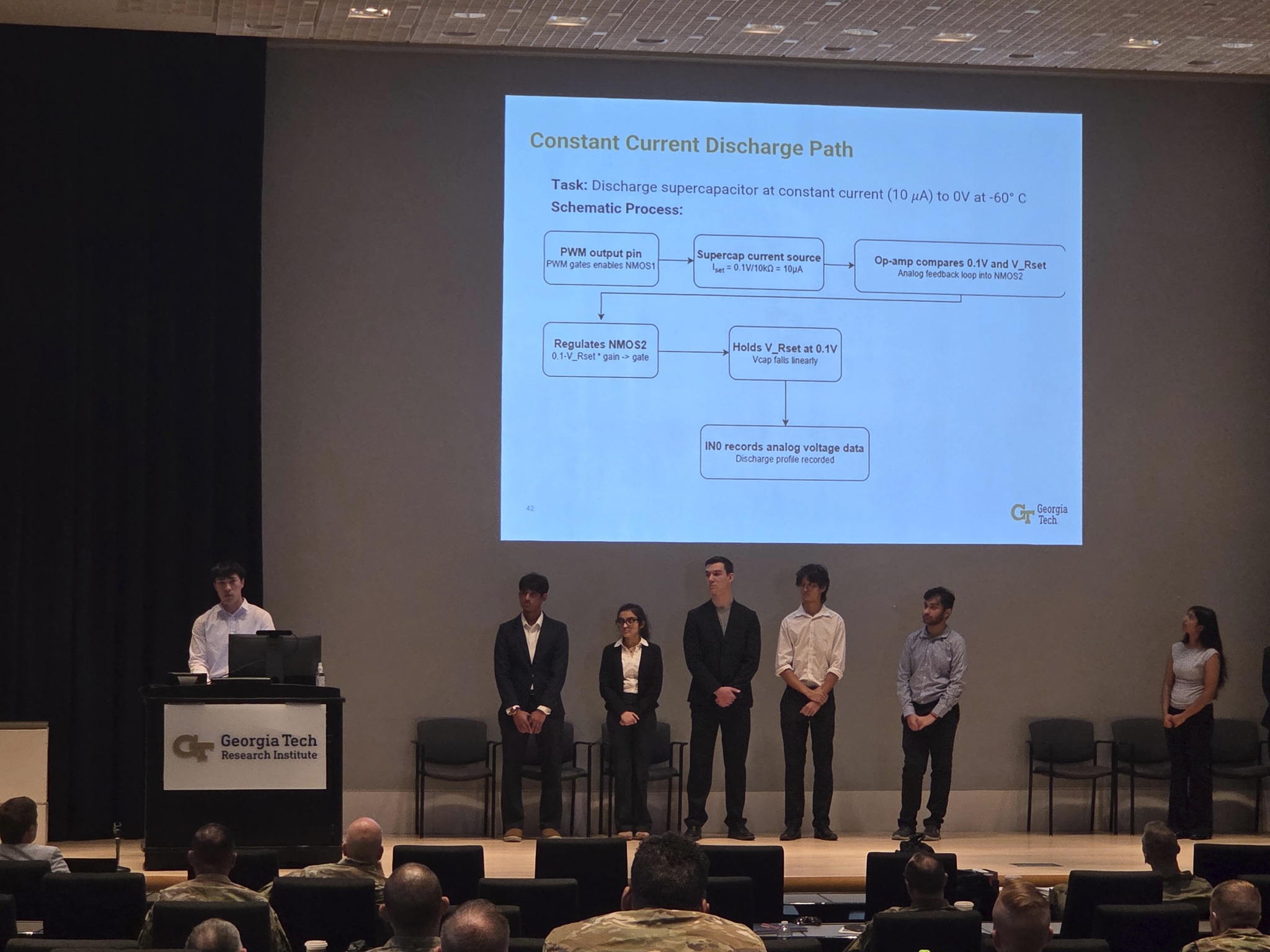
NMOS1 connects directly to the microcontroller through a connector pin TX_MOSI_D1, which is coded as a pulse wave monitor that enables the discharge path when high. The current is set by R7 (9kΩ). With a 0.1V reference, the target voltage across R7 is 0.1V, giving I = 0.1V / 9kΩ ≈ 11µA ≈ 10µA (with NMOS propagation delay). TSZ901ILT2 is an op-amp that compares this 0.1V reference against the actual voltage developing across R7 and drives the gate of NMOS2 to correct any deviation: if current rises, NMOS2 is turned down; if it falls, NMOS2 is turned up. This feedback loop is what maintains constant current and ultimately produces a linear voltage decrease.
The transient simulation confirms the circuit behaves as designed. Note: the simulation was run on an earlier version of the schematic: R1 in the simulation corresponds to R7 in the current schematic. I(R1) holds at 9.99µA throughout each discharge phase, validating the feedback loop. The voltage (blue trace) decreases linearly during discharge. When the voltage jumps sharply back up, that represents the capacitor being fully charged again before the next discharge cycle begins. The green trace shows the control switching signal driving this charge/discharge cycling.
Monitor Current & Monitor Voltage
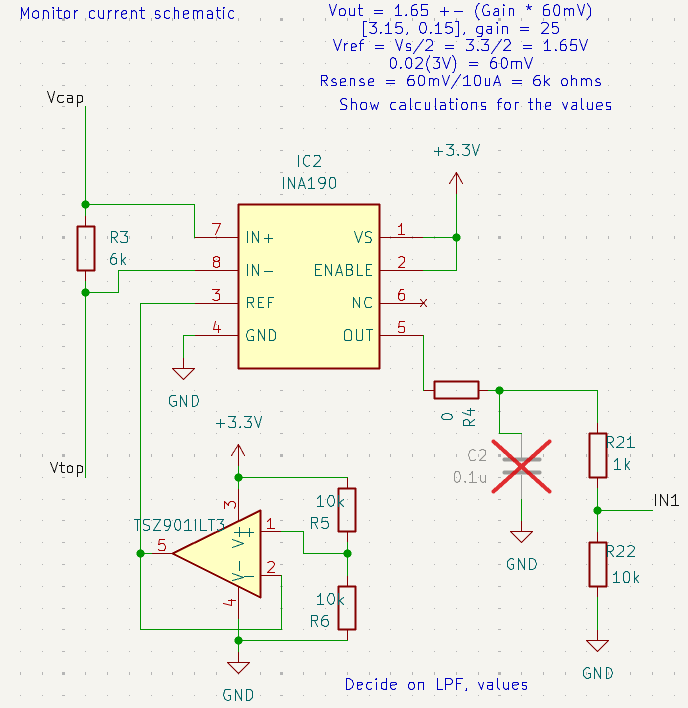
Current monitoring: For current monitoring, we use the INA190 bidirectional current sense amplifier. It introduces minimal voltage drop into the path and outputs an analog voltage proportional to current, which the STM32 converts to a digital reading.
R3 (6kΩ) is the shunt resistor, sized by the expected voltage drop: V = I * R, so 60mV = 10µA * 6kΩ. The INA190 reads the differential voltage across IN+ and IN-, multiplies it by a gain, and adds it to a reference voltage. The 1.65V reference is generated by a TSZ901ILT3 op-amp buffer configured with equal resistors (R5/R6 = 10kΩ each), centering the output at half of 3.3V. This reference is necessary because the INA190 is bidirectional: positive current produces a reading above 1.65V and negative current produces a reading below. Without it, negative current would collapse to 0V and produce unusable data.
The output equation for IN1 is: Vout = Vref + (Gain * Vsense) = 1.65 + (25 * 60mV) = 1.65 + 1.5V = 3.15V (at +10µA) = 1.65 - 1.5V = 0.15V (at -10µA). We selected the INA190A1 variant for a gain of 25.
A DNP (Do Not Populate) low pass filter is included on the output to suppress noise if needed after testing. Because the output reaches 3.15V and the STM32 ADC accepts up to 3V, we step it down with a voltage divider: V_IN1 = Vout_INA * (10k / 11k) = Vout_INA * 0.909.
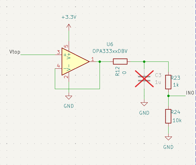
Voltage monitoring: For voltage monitoring, we use the OPA333 op-amp in unity-gain configuration. It reads the supercapacitor voltage and presents it as a signal to the STM32 via IN0. As with current monitoring, a DNP low pass filter is included if fluctuations appear during testing, and a similar voltage divider steps the signal down to stay within the 3V ADC limit.
Since neither chip is in the KiCad library, both symbols and footprints were created manually from their datasheets. Simulation is not possible without a KiCad SPICE model, so measured values will be validated during post-fabrication thermal testing.
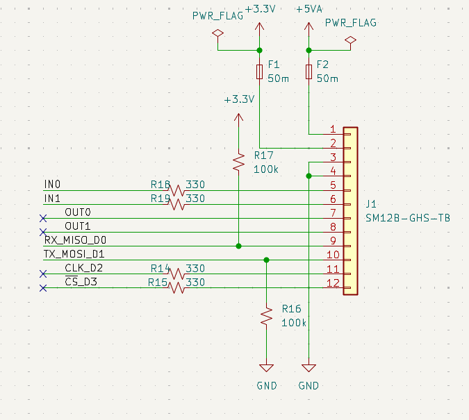
MCU Connector
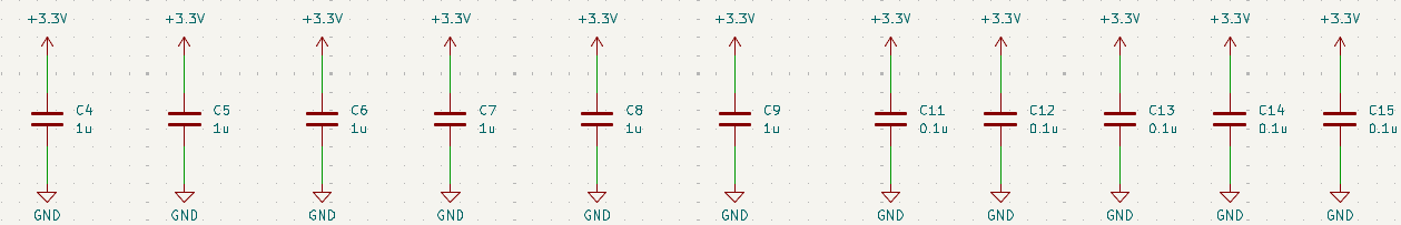
The schematic also includes decoupling capacitors at the power inputs to every chip. These filter transient voltage fluctuations and ultimately reduce noise on the supply lines to our components.
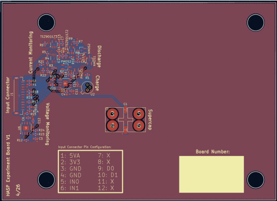
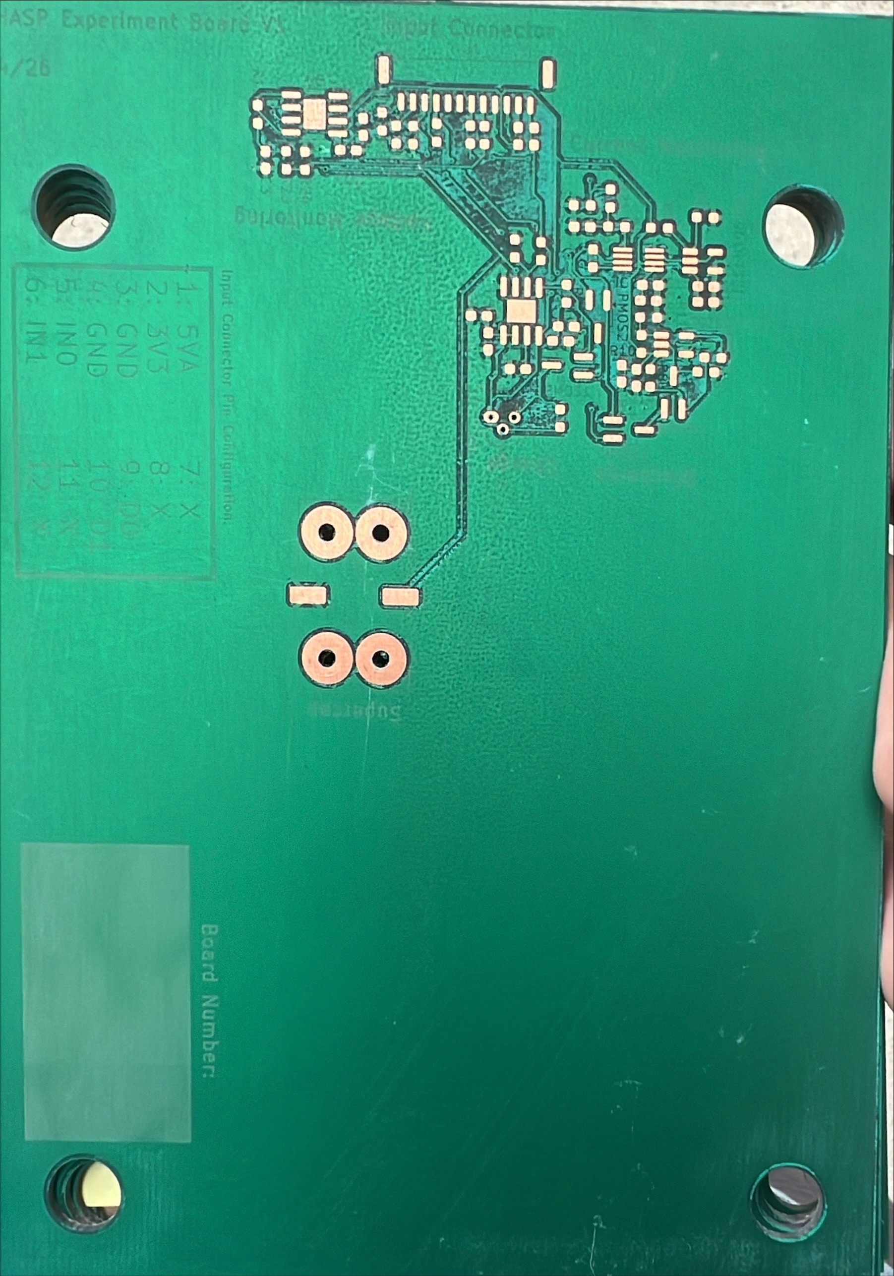
Routing, Footprints, Design and Electric Rule Checks
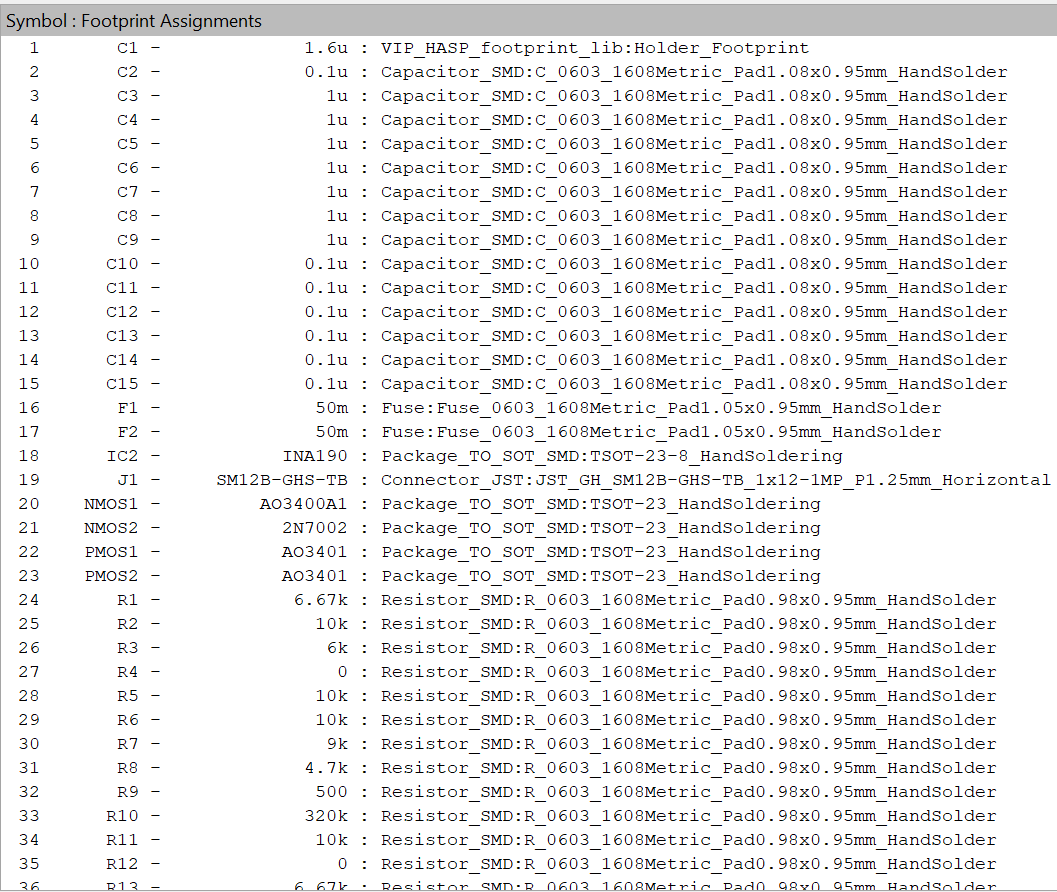
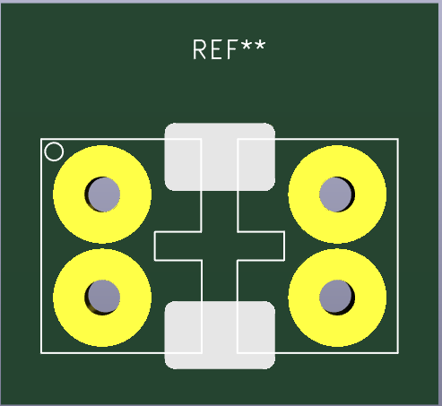
All components have footprints either pulled from the KiCad library or created manually. Our supercapacitor holder is an example of a custom footprint, built by a team member from the physical dimensions of the actual physical supercapacitor holder.
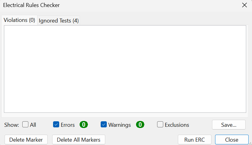
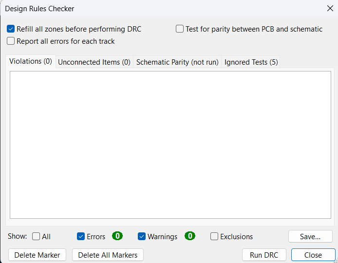
PCB routing connects all power nets to their respective supply pins and GND pins. Decoupling capacitors are placed as close as possible to each chip's supply pin to minimize noise. Once routing is complete, a Design Rules Check (DRC) verifies no layout violations exist.
Future Work
Since this project is run through Dr. Ready's lab at the Georgia Tech Research Institute, our team had the opportunity to present our research and findings to an audience of United States Space Force, including Chief Master Sergeant John F. Bentivegna and other active-duty members. Presenting work that may one day be used in space applications to the people who operate in environment was an experience unlike any other.
Outcome
[Results will be added following the NASA balloon flight in August 2026.]